Optimizing performance of your CUDA code
Recap of the obvious:
- Latency hiding by maximizing occupancy (playing with your
blockDim,gridDim).- Careful though how much shared memory (or register memory) you assign per block (resp. per thread) as it might lower your occupancy.
- Data reuse, Shared memory usage and tiling.
- Minimizing control divergence (high SIMD utilization).
DRAM bank:
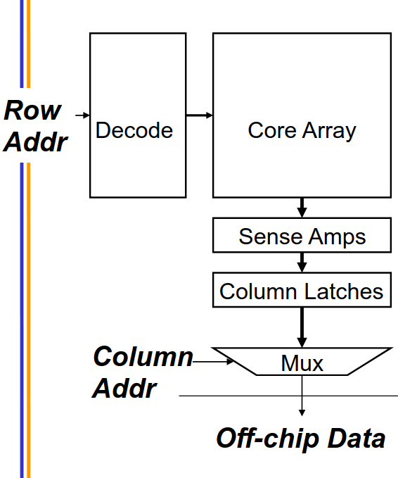
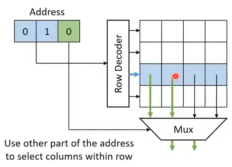
On a higher level, a DRAM bank (sketched above) does the following:
-
The incoming row address is decoded by the Row Decoder, which activates the corresponding row in the DRAM array.
-
The contents of that row are sensed and amplified by the Sense Amplifier, temporarily stored in Column Latches.
-
The Column Latches are then passed through a multiplexer (MAX) where the specific columns are selected based the Column address.
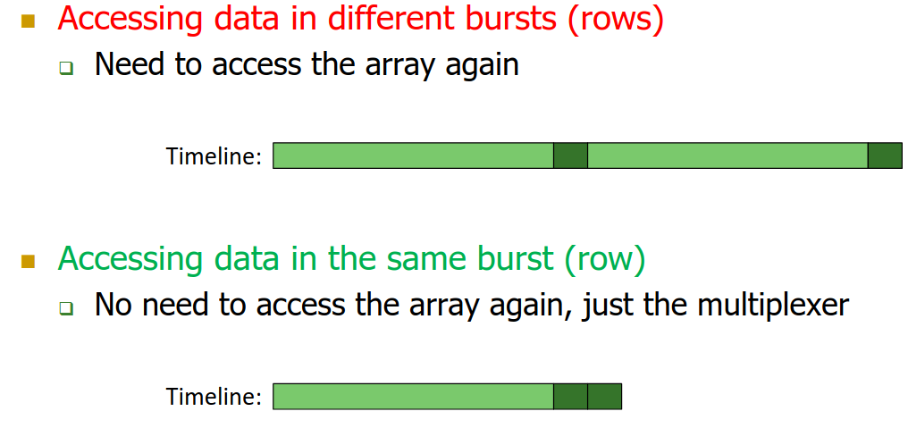
The key factor here is that if the next access corresponds to the same row address, then we can save the latency of Step 1 and Step 2 (which are the longest ones), and directly jump to Step 3, by fetching the necessary column from the Multiplexer. This is called a memory coalesced access.
Memory coalescing on GPUs:
-
Memory coalescing is when threads within the same warp access consecutive elements in the DRAM burst (hence, saving latency), and only one DRAM transaction would be needed.
- Again, always keep in mind how threads (within a block) are mapped into warps, and that
threadIdx.xis the fastest moving dimension, followed bythreadIdx.y, and thenthreadIdx.z:- For a 2D block,
tid = threadIdx.x + blockDim.x*threadIdx.y. - For a 3D block,
tid = threadIdx.x + blockDim.x*threadIdx.y + blockDim.x*blockDim.y*threadIdx.z.
- For a 2D block,
- More on this here: Memory coalescing and block indexing.
Let’s see a few examples of code
int idx = blockDim.x*blockIdx.x + threadIdx.x
C[x] = A[idx] + B[idx]
Banked memories and channels:
-
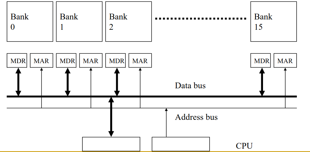
The idea is to split memory into multiple banks that could be accessed simultaneously, but share the same buses. Or into independent channels that have separate data buses. One should be careful though of bank and channel conflicts.
-
Latency can be easily hidden with multiple banks. While
bank-xis busy opening a row, another row frombank-ymay already be ready for transfer. Hence why it’s good to aim for high occupancy.
-
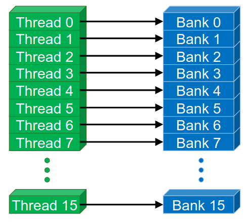
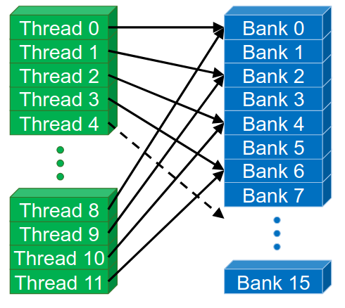
Shared memory is a banked memory: Successive 32-bit words are assigned to successive banks (generally 32 banks in total).
-
Bank conflict can only happen within a warp, as all threads within a warp execute in lockstep.
- Reducing bank conflicts:
- Padding.
- Randomized access.
Other important considerations:
- SIMD utilization
- Avoid divergence when possible.
- Code in warp-minded way (
if (threadIdx.x < 32) {...})
- Atomic Operations: useful to prevent data races.
- If two different warps within the same block are trying to access the same memory location (shared or global).
- Useful to sync, coordinate threads running together.